The basic information of LED light emitting chip should be collected!
The core light-emitting chip in LED products belongs to the semiconductor industry, and currently the largest in China belongs to Sanan Optoelectronics. What information does the chip of this crucial country's core technology contain? What are some of its basic characteristics? Let's take a look together.
The general production process flow of the chip: thinning ---- evaporation ---- lithography ---- cutting ----- test. These main processes include up to dozens of small processes, and the equipment technology of each process is extremely complicated and precise. We briefly describe the production process of GaN.
First, the gallium nitride (GaN) -based epitaxial wafer was fabricated on the substrate. This process was mainly completed in a metal organic chemical vapor deposition epitaxial wafer furnace (MOCVD). Commonly used substrates are mainly sapphire, silicon carbide and silicon substrates, as well as GaAs, AlN, ZnO and other materials.
Then, the two electrodes of the LED PN junction are processed. The electrode processing is also a key process for making LED chips, including cleaning, evaporation, yellow light, chemical etching, fusion, and grinding; then scoring, testing, and dividing the LED wool Select, you can get the required LED chip. If the chip cleaning is not clean enough, and the vapor deposition system is not normal, it will cause the metal layer (electrode after etching) that is evaporated to fall off, the appearance of the metal layer is discolored, and the gold bubble is abnormal.
In the front-end process of the chip, tweezers must be used for various processes such as cleaning, evaporation, yellow light, chemical etching, fusion, grinding, etc. There will be scratches on the chip electrodes.

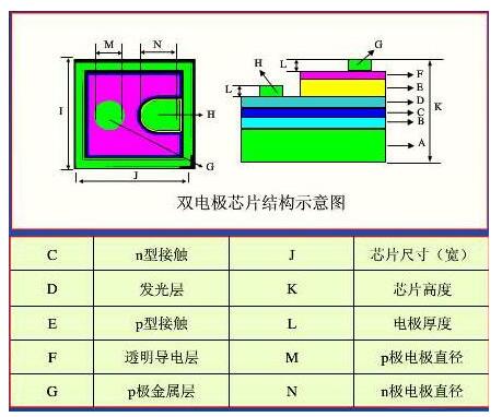
What is the general structure of the chip? The diagram is as follows:

Here is a brief description of the chip:
1. The basic structure of the chip is composed of four parts: pad, P, N and base. The light emitting part is the junction of P and N (the PN junction area)
2. The material of solder pad is generally aluminum pad or gold pad.
3. The bottom of the base is generally uneven and carved with gold.
4. Chip size varies by supplier.
There are three types of chip components: binary, ternary and quaternary. The few yuan here are mainly about the elements that make up the chip. If two elements are binary, three elements are ternary. We list the commonly used binary, ternary, and quaternary chip types. Most of the early-stage and current Taiwan-funded chips are still ternary and ternary chips, while domestic chips are mainly quaternary chips. The quaternary chips are far superior to the ternary and ternary chips in terms of brightness and unit price.
Binary: GaN, GaP. Commonly used chips: C430-CB290-E1000, ED-011YGU, ED-013YGU, ED-010RN, ED-011RD, etc.
Three yuan: InGan, GaAIAS, GaASP. Commonly used chips: C470-CB290-E1000, C505-CB290-E1000, C512-CB290-E1000, C525-UB230-E1000, etc.
Quaternary: AlGaInP commonly used chips: ES-CAYL512, ES-CASO512, ES-CAHR512, ES-CASR512, UED-712SYS-MV, ES-CAYO512, UED-712UR-V, UED-712SO-V, etc.
Chip main performance indicators: Vf, Iv, Wd
(1) Vf: Vf factors affecting chips in different regions are:
A. Uneven distribution when evaporating material
B. Uneven annealing temperature
(2) Iv: Influencing factors see luminous efficiency
(3) Wd: The effect is: material and ratio
(4) The relationship between Vf and Wd: Wd = 1240 / Vf (nm)
Note: The energy band of the blue active layer is 2.7v. However, due to the influence of Si doping and the contact of the pad metal, the frontal voltage is 3.8v at 20mA. As long as the four-piece structure and doping level are improved, the lower than The positive voltage of 3.0v. The voltage part of the blue emerald chip currently produced is already lower than 2.8v. This point is mainly for the chip manufacturers to improve the internal quantum luminous efficiency, reduce the material resistance, and make the current distribution more uniform. Improvement of voltage.
